Current location:Home > Application area
Published on:2021-05-05 15:43:27Views:14048【Smallinlarge】
In 2019, the amount of investment made in Chinese semiconductor industry was approximately RMB 30.00 billion Yuan, and increased to RMB 140.00 billion Yuan; in 2021, the total amount of investment made by Chinese semiconductor enterprises in production lines reached RMB 190.00 billion Yuan.
This year, the demand for semiconductor element terminal is increasing, the market prosperity of electric vehicles, Internet of things, photovoltaic energy storage, and other markets remains optimistic, and the demand for power, RF and other application platforms is booming.
The wide band-gap semiconductors represented by SiC/GaN have been widely used in 5G communications, automotive electronics, quick charging, and other fields gradually. As the key consumables for precision and ultra-precision processing procedures, the agglomerated diamond grinding materials manufactured by Zhongji Micro Material play a crucial role in the grinding process in semiconductor industry.
|
Recommended Particle Size |
Diamond Agglomerated Powder |
Diamond Agglomerated Grinding Fluid |
Alumina Polishing Fluid |
Silicon Oxide Polishing Fluid |
|
3-8μm |
2-5μm |
5-20μm |
60-120nm |
|
|
8-12μm |
3-6μm |
|
|
Due to its characteristic of spherical multi-edge angle, the ball-like agglomerated diamond grinding material can maintain the high grinding force without scratch during the process of grinding and polishing. It is widely used for grinding of the hard and brittle materials such as sapphire, silicon carbide, and gallium nitride.
It has the ball-like shape feature, presenting multi-edge structure in microscope view, and showing slight luster of natural mineral;
It has higher cutting capability, and guarantees high precision polishing effect;
It has narrow distribution range of particle size, so as to achieve uniform surface roughness;
It has stable quality of products, and small difference between batches;
It can achieve ultra-high purity.
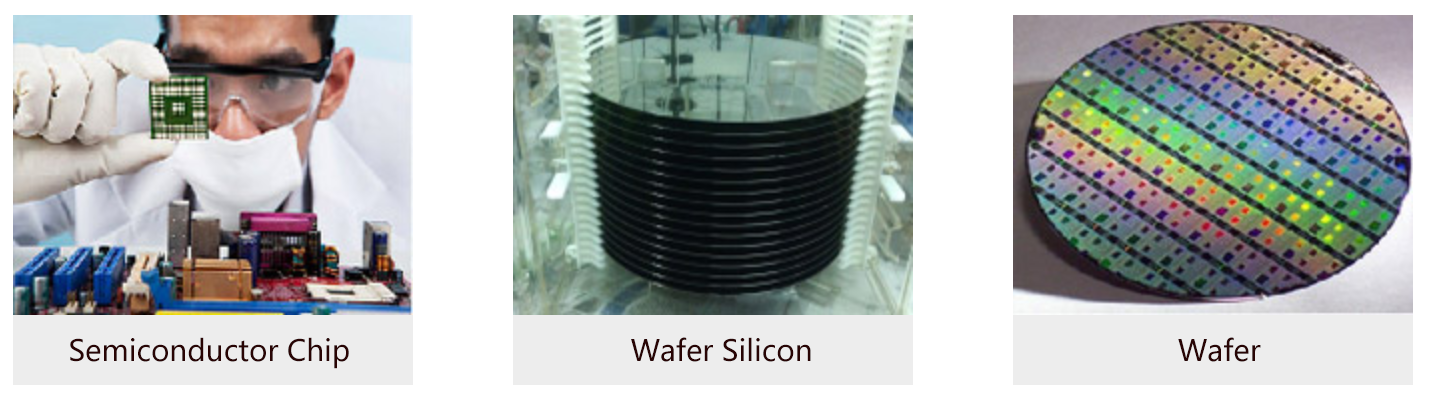
Suitable for processing of semiconductor: Grinding of semiconductor materials such as silicon wafer, germanium, gallium arsenide, indium phosphide, silicon carbide, and gallium nitride;
Processing of metal materials, such as stainless steel, die steel, titanium alloy, and other metal materials.
Polishing of sapphire optical chip, LED sapphire substrate, watch lens, crystal, gem optical lens, optical glass, quartz, and silicon wafer of optical fiber and of photovoltaic enterprise; polishing of germanium sheet, polishing of gallium arsenide; polishing of indium phosphide; polishing of zinc selenide; polishing of optical fiber connector; polishing of optical fiber patch cord; polishing of glass;
For recommended products or technical support, please contact our application engineers.